Imagine a material as thin as a whisper, bendable like a leaf, yet capable of generating electricity from the gentlest touch, the flutter of a butterfly's wing, or the pulse in your own wrist. Now, imagine manufacturing this wonder-material across vast, dinner-plate-sized sheets with the precision of a computer chip factory.
This isn't science fiction; it's the cutting-edge reality of wafer-scale heterostructured piezoelectric bio-organic thin films. It's where the elegant machinery of biology meets the powerful scale of advanced manufacturing, promising a future of smarter, more sensitive, and sustainable electronics.
Piezoelectric Power: Nature's Silent Spark
At the heart of this technology lies piezoelectricity (from the Greek "piezein," meaning to press or squeeze). Simply put, certain materials generate an electrical charge when you squeeze, bend, or stretch them. Conversely, applying electricity makes them physically move. Quartz in watches and lighters is a classic, but rigid, example.
The Bio-Organic Advantage
Nature excels at building complex, efficient nanomachines. Proteins like those in spider silk, bone, or even specific viruses possess inherent piezoelectric properties.
- Biocompatibility: They integrate safely with living tissue
- Biodegradability: They can break down naturally
- Superior Flexibility: They bend and flex far better than ceramics
- Nanoscale Precision: Biology builds with atomic-level accuracy
Heterostructures: The Power of Layers
A heterostructure is like a high-tech sandwich. It combines layers of different materials, each chosen for specific properties.
Wafer-Scale: The Manufacturing Leap
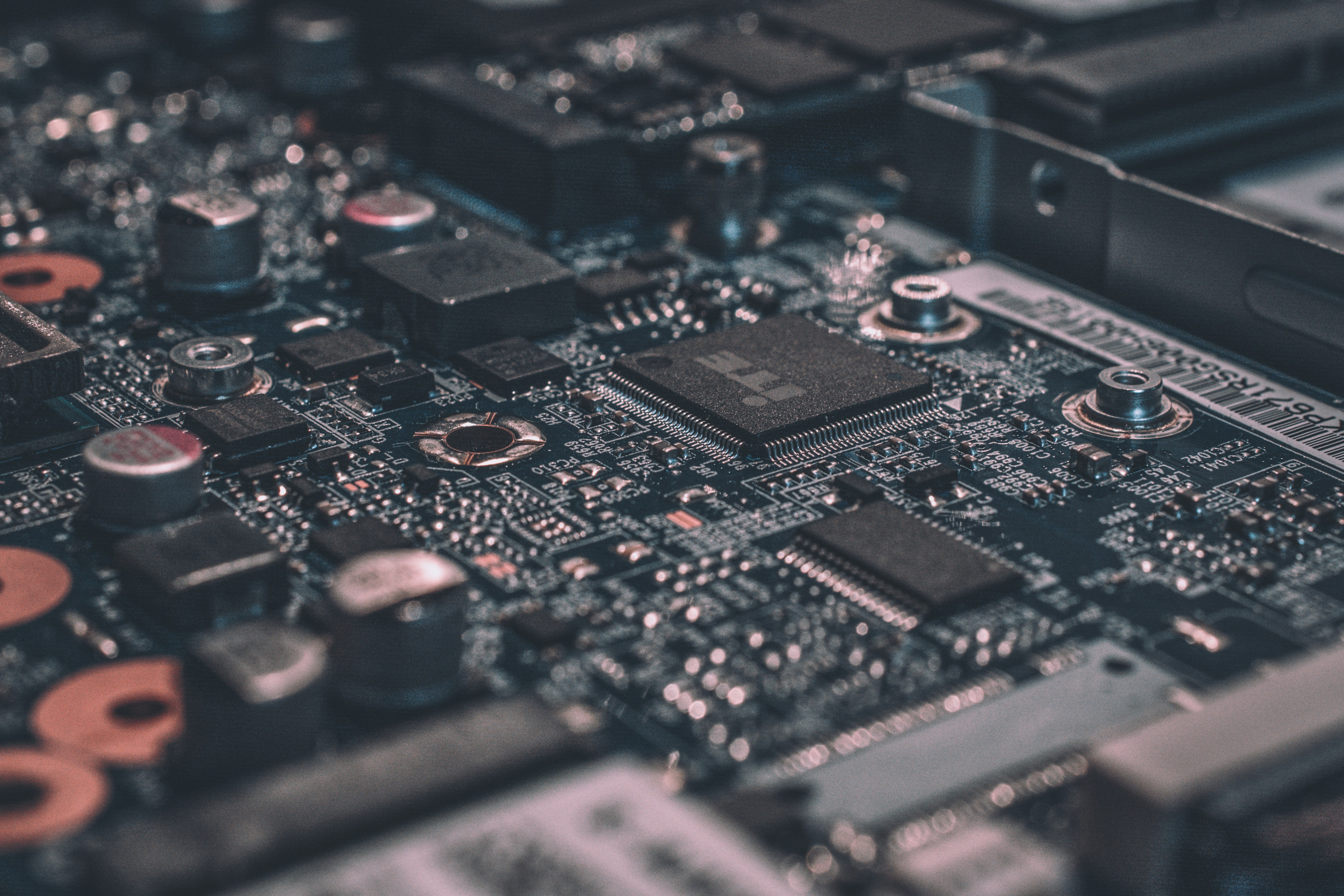
Traditionally, working with delicate biological materials meant tiny, lab-bench samples. Wafer-scale refers to manufacturing these complex bio-organic heterostructures on large, round silicon wafers (like those used for computer chips). This leap is crucial for moving from lab curiosities to real-world applications.
The Breakthrough Experiment: Engineering Virus Power on Silicon
One landmark experiment, often cited as a blueprint for this field, involved using a harmless virus called the M13 bacteriophage to create wafer-scale piezoelectric films.
Phage Farming
Billions of M13 bacteriophages were cultivated in bacterial cultures. These viruses are rod-shaped and naturally piezoelectric due to the precise arrangement of proteins in their coats.
Alignment is Key
The critical step was controlling how these nanorods lay down. Researchers used a technique called "flow-assisted alignment" during spin coating to align the rod-shaped viruses in parallel over the entire wafer surface.
Building the Sandwich
Multiple layers were built: aligned phage film, conductive layers, and electrodes, creating a functional heterostructure.
Testing the Power
The finished wafer was diced into devices and tested under various mechanical forces, temperatures, and bending cycles to evaluate performance.
Data & Analysis: Proof of Scalable Bio-Power
Piezoelectric Performance Comparison
| Material Type | Example | d₃₃ (pm/V) | Flexibility |
|---|---|---|---|
| Ceramic | PZT, Quartz | 200-600 | Rigid |
| Synthetic Polymer | PVDF | 20-30 | Flexible |
| Bio-Organic (Virus) | M13 Bacteriophage Film | 30-50+ | Highly Flexible |
Wafer-Scale Production Metrics
| Parameter | Result |
|---|---|
| Wafer Diameter | 4-inch or 6-inch |
| Film Uniformity | >90% Consistency |
| Layer Thickness | 100 nm - 1 μm |
| Device Yield | High (>80%) |
Measured Device Performance
| Test Condition | Measured Output | Key Insight |
|---|---|---|
| Light Finger Tap | 0.5 - 2 V | High sensitivity |
| Low-Frequency Bend | 1 - 5 V | Effective energy harvesting |
| Bending Cycles | <10% Degradation | Excellent durability |
The Scientist's Toolkit: Building Bio-Electronic Wafers
Creating these films requires a fascinating blend of biology and engineering:
M13 Bacteriophage
The core piezoelectric "engine." Genetically engineered variants can optimize charge generation or binding.
Silicon Wafer
The ultra-flat, rigid substrate providing mechanical support and compatibility with microfabrication tools.
Atomic Force Microscope
Used to image the nanoscale structure of the film and directly measure its local piezoelectric properties.
Spin Coater
Instrument that spins the wafer at high speed to spread solutions thinly and evenly, crucial for film uniformity.
A Flexible, Sensitive Future
Wafer-scale heterostructured piezoelectric bio-organic thin films are more than just a scientific marvel; they represent a convergence point. They harness the exquisite efficiency and biocompatibility of nature's designs and combine them with the scalability and precision of modern electronics manufacturing.
Future Applications
- Biodegradable health monitors
- Smart clothing generating power
- Large-scale sensor networks
- Neural interfaces

The Path Forward
The silent spark of piezoelectric biology is finally ready to shine on the big stage. By learning to build with nature's blueprints on an industrial scale, we are opening the door to a new generation of electronics that are not just smart, but also soft, sustainable, and intimately connected to the world – and us – they serve.